Enables concurrent connection to 3 different security systems
TOKYO — (BUSINESS WIRE) — June 24, 2013 — Toshiba Corporation (TOKYO:6502) today announced that it has launched an NFC controller LSI (CLF[2]) "T6NE2XBG" for secure mobile payments via proximity wireless communication. Mass production is scheduled to start in October.

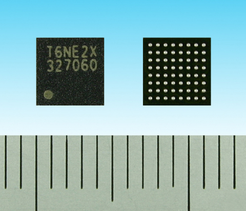
Toshiba NFC controller LSI "T6NE2XBG" (Photo: Business Wire)
The market for mobile payments, using smartphones and other mobile devices in transactions, is growing. The T6NE2XBG enables multiple concurrent connections with three different secure elements (SE[3]), allowing manufacturers to design NFC-enabled applications before the SE for the transaction system is determined.
Toshiba has shipped more than 400 million custom LSIs for proximity cards and mobile payment systems, and expertise in RF[4] technology gained through this experience is integrated in the new product. Toshiba is also developing an LSI for embedded SE, and plans to introduce a packaged product that incorporates CLF and SE.
A demo board of T6NE2XBG will be displayed at the Mobile Asia Expo 2013, to be held at Shanghai from June 26th to 28th.
Features
1. Concurrent connection to up to three multiple SEs
A range of SE are being deployed into applications to meet the different requirements of payment system operators. The new product enables multiple concurrent connections to a maximum of three different SEs, making it possible to design applications before the system SE is finalized. The product also supports thee different communication protocols to SEs.
2. Integrated circuit to adjust RF connectivity
Manufacturers need to adjust RF connectivity of NFC-enabled devices to receive necessary certification that payment system operators require. The product integrates an adjustment circuit and records each parameter into embedded EEPROM, which enables adjustment of each operating mode (card emulation, reader writer, and P2P[5]) and different RF modulation options (Type A, B and F).
Applications
Smartphones, tablet terminals, NFC readers/writers, and home appliances with wireless communication functions
|
Features of the New Product |
||||||
| Part Number | T6NE2XBG | |||||
|
Sample Price
(Tax Included) |
300Yen | |||||
| Mass Production | October, 2013 | |||||
| Mass Production Volume | One Million pcs per month | |||||
| Main Features | CPU: | ARM Cortex™-M0 [6] | ||||
| Max Operation Frequency: | 27MHz | |||||
| Communication I/F: | RF: |
ISO14443 TypeA/B,
|
||||
| Host I/F: | SPI I2C UART (option) | |||||
| SE IF: | 3×SWP UART SPI (select 3 interfaces) | |||||
| Antenna Drive Current: | 64mA (max value and settable step by step) | |||||
| Power Dissipation: |
Stand-by: max 5μA, Card mode: max 5mA,
R/W mode: max 10mA (antenna drive current excluded) |
|||||
| Supply Voltage: | 2.5V~3.3V (3 mixed power supply voltage) | |||||
| Package: |
BGA64
|
|||||
| Operation Temperature Range: | -30 to 85 degC | |||||
|
CLF
Embedded Software |
NFC Forum: | NCI Ver1.0 (2012/11/6) compliant | ||||
| EMVCo: | Book D EMV contactless communication protocol specification Ver. 2.2 compliant | |||||
| 3 Secure Element I/F: | Application ID/Technology/Protocol base routing | |||||
| Notes | ||
| [1] | NFC: Near Field Communication. One of the international standards for proximity wireless communication system. | |
| [2] | CLF: Contactless Front-End. A kind of NFC controller. | |
| [3] | SE: Secure Element. Semiconductor products which has security functions against masquerading attacks from outside. | |
| [4] | RF: Radio Frequency. | |
| [5] | P2P: Peer-to-pear. Communication systems that the either side can initiate a session and has equal responsibility. | |
| [6] | ARM is a registered trademark and ARM Cortex is a trademark of ARM Limited in the EU and other countries. | |


